(this document is simply the expanded version of the zipfile found here, and has no modifications other than this message have been made to Joe Clussman's work)
The available documentation on the TI-86's link port is relatively comprehensive, although scattered and sometimes confusing or contradictory. However, there has not been a complete document to date that properly addresses the method of programming for the link port in Z80 assembly language. Here is my attempt at an understandable "all you really need to know" document. Alas, this document comes at a time when programming for the TI-86 is pretty much dead. And unfortunately, there weren't as many multiplayer games as there ought to have been...
The TI-Link port allows for asynchronous serial communication to and from the calculator. The port works off of the standard TTL signal levels (0 Volts and +5 Volts). The link cable is composed of three conductors: two Signal wires and one Ground wire which serves as a voltage reference. Data bits can only be transferred in a single direction at any given moment. There is a standard protocol which governs the communication from one calculator to another calculator, a Personal Computer, or a CBL/CBR.
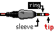
The TI-Link cable connector is a standard 2.5mm "stereo jack." The three connections on the jack are called the tip, ring, and sleeve. And the fancy coloring does serve a purpose disclosed shortly below.
The link cable is wired "straight-through," versus being a "crossover" cable. This means that the tip of one connector is wired to the tip of the other, and so-on.
Now about those fancy colors-- cut away the rubber coating on the link cable, and three internal wires will be found. The colors of the insulation on those wires are red, white, and black (or bare copper wire). The white wire connects up with the "ring" and the red one connects to the "tip." And since the white and red wires have no official names, they'll just simply have to be called the "White" and "Red" wires.
Below is the schematic for the link portion of the TI-86 calculator.
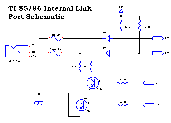
Although not shown, inputs LP1 and LP2 are connected to two outputs coming from the Z80-instruction compatible CPU, and outputs LP3 and LP4 are connected to two inputs going into the CPU. Notice I stated "Z80-instruction compatible CPU," because it is not a true Z80 processor-- its not even manufactured by Zilog, but by Toshiba! This custom CPU contains "on-chip" ports which allow for this kind of a direct connection.
Diodes D7 and D8 are present to protect the inputs to the port on the CPU from an excessive positive voltage from the jack. However, these diodes do little to protect the CPU from negative polarity. (If a sustained negative voltage, even as low as -3V, were allowed directly into the CPU, it would most likely be damaged.)
Then there are the "fuse-links," which are actually really low value resistors, maybe 0.1 Ohm. In the event of a negative voltage causing excess current, they'd probably be the first to blow, hence their name. But maybe they are just used as jumpers, as the source I based the picture on suggested.
Transistors Q6 and Q7 are used to amplify the signal coming from the CPU, and the 471 Ohm resistors protect those transistors from sinking excessive current in normal operation.
As stated before, wires LP1 and LP2 are connected to outputs from the CPU. The signal coming from the CPU is digital, either a zero or a one. Let's just focus on one of the two identical output circuits. A zero (0V) at the base (B) of the transistor will not turn it on, allowing a weak +5V to pass through the 10K Ohm resistor and diode, and appear at the signal output of the jack connector. A one (+5V) at the base of the transistor, however, will turn it on. This will drop the signal output at the jack connector to very near 0V, because the pull-up current will flow through the 10K Ohm resistor, the diode, 471 Ohm resistor, and NPN transistor to Ground.
To get even more technical, this output circuit is called an Inverter or NOT circuit. Why? Because the output is the reverse of the input. Also, it is Open-Collector, because the collector (C) of the transistor is used as an output and is not connected to another transistor, but is instead being supplemented by a weak pull-up resistance to get that output to the positive level. That and the fact the output can be shorted to ground without any damage... Whoah... Did I just lose you? I hope not, because it's important.
Now that we got the sending of information out of the way, let's try the input section. (I swear, it's not that complicated!) Right now, we don't have anything connected to the jack, and we'll say that the two NPN transistors are off. A +5V will flow through the 10K resistors and into two inputs of the CPU through LP3 and LP4. The CPU will read the state of the two inputs as a binary ONE.
Let's turn the NPN transistors on again, diverting the pull-up current through them. The voltage at LP3 and LP4, as well as the output at the connector, will also sink down to near 0V. Thus the CPU will read the state of LP3 and LP4 as a zero.
What if another TI-86 is connected to this circuit one using the link cable? This other calculator can drive the signal wires at the jack either high or low, +5V and 0V respectively, using this exact same circuit. There are four possible states...
If one wants to interface a circuit to the TI-86 link port to a digital output, two rules should be followed:
With the technical details of the hardware out of the way, the focus can finally shift to the software aspects.
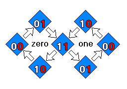
Note again that the inactive state is both lines at a binary one (+5V). Now for an explanation of how either a zero or a one is sent:
When sending a zero bit:
When sending a one bit, the process is the reverse:
Simple, effective, and it works out quite well in a system where accurate timing is unavailable and outside EMF interference is not too high...
Now, it's evident that a single bit can be sent, but sending just a single zero or one is useless. In practice, the communication sends eight of these bits at a time, followed by a short wait. This, of course, is a data byte. The transmitting end of the link sends the lowest significant bit (LSB) first, ending with the most significant bit (MSB).
A byte itself is still pretty useless, so a whole series of bytes are sent, which composes a data packet. You can find more about this is in the TI-LINK Protocol section.
Transfer rates are typically around 45 to 50 Kbps, and the timeout period for a receive error is supposed to be 3 seconds.
Port 7 is where the link port data can be accessed directly from an assembly program. Data is written to and from port 7 with the OUT and IN instructions, respectively. The table below contains the test data obtained with the "Internal Link Test" Program.
| Wrote To Port | Physically Measured | Port Read | ||||||||
|---|---|---|---|---|---|---|---|---|---|---|
| Value | ?? | OT | FF | IN | WHITE | RED | ?? | OT | FF | IN |
| $FC | 11 | 11 | 11 | 00 | 0V | 0V | 00 | 00 | 11 | 00 |
| $E8 | 11 | 10 | 10 | 00 | 0V | +5V | 00 | 00 | 10 | 01 |
| $D4 | 11 | 01 | 01 | 00 | +5V | 0V | 00 | 00 | 01 | 10 |
| $C0 | 11 | 00 | 00 | 00 | +5V | +5V | 00 | 00 | 00 | 11 |
Note the following things about the above table:
Bit 5 controls the White wire, and bit 4 controls the Red one. Notice how things get inverted. Take for example the last row where the value $C0 is written, both the White and Red wires rise to +5V. All of the TI-86 programs whose sources are available seem to use the instructions below to change the logic levels of the wires:
        ld A,$C0      ;White wire +5V, Red Wire +5V
        out (7),a
        ld A,$D4      ;White wire +5V, Red Wire 0V
        out (7),a
        ld A,$E8      ;White wire 0V, Red Wire +5V
        out (7),a
        ld A,$FC      ;White wire 0V, Red Wire 0V
        out (7),a
Bit 1 is the status of the White wire, and bit 0 is the status of the Red wire. To read the status simply get the value from port 7, mask off the other bits, and then use a compare instruction as in the example below.
        in A,(7)
        and %00000011       ;Only bits 1 and 0 matter
        cp 0                ;In this case check for both being at 0V.
Like so many other forms of data transmission, the link port protocol uses command/data, acknowledgment, and end-of-transmission packets.
The packet is composed of the following:
The Machine ID tells what device is sending the data. A value of $86 (hex digits) is, as you may have guessed, the TI-86 calculator; and a value of $06 is the Graph-Link software expecting a TI-86 on the other end. Follow the pattern for the other calculators. An upper nibble of A-F has never been observed, so perhaps one could use this to differentiate a software program.
The command byte tells what this packet is all about. Some examples are: an acknowledge packet has a command byte of $56, $15 means just data, and $5A indicates a checksum error. There are other values, and if interested refer to the TI-86 Link Protocol and Variable Format Guide by Tim Singer
This gives the length of any data to follow. A value of $0000 indicates NO DATA and therefore no data bytes or checksum is to follow. If the value is non-zero, it can be in the range of 0-65535 bytes. One byte of data would be sent in the order of $01 then $00 in low-byte then high-byte format. That 16-bit value is the reason why those group files are limited to around 65000 bytes.
This is a string of bytes representing something, whether it be a floating point number, string, or program. If this is any named variable (like what would be found in the VAT), a 12-byte variable header would come before the actual data.
This is the 16-bit wrap-around unsigned sum of all the bytes in the data section. It is sent as low-byte then high-byte format.
In the Graph-Link Software, there is an option to get what is currently displayed on the calculator's screen. When the button is clicked, the software sends a command packet to the TI-86 composed of $06, $6D, $00, $00. The TI-86 responds with an acknowledge of $86, $56, $00, $00, and then sends a data packet of $86, $15, $00, $04, [1024 bytes of screen], [16-bit checksum]. The software then acknowledges back with $06, $56, $00, $00.
The operating system does not use the previous state as stored in bits 2 and 3 of port 7. Furthermore, it will attempt to use its own routine when it detects a 0V on either of the lines. If this happens inside your assembly program it will hang the calculator.
Therefore, your assembly program must be sure to set the lines back to the +5V state by OUTing a value of $C0 before exiting. But it gets a little worse, as routines like _getkey check for link port activity, and again, if both the data lines are not at +5V, the function will hang.
Do not assume that your transmissions will be error free. Maybe not from the errant cosmic particle that comes zipping from Epsilon Eridani, but from the simple fact that some friend could come along and yank the cable in the middle of transmitting a byte.
In addition, transmission tends to get a little bit flakey when the battery level is low. In programs that extensively use the link feature, checking the battery level upon starting the program would be a good idea.
Thus, a robust program would have timeouts, some sort of checksum calculation, and battery level measurement to ensure proper error detection and recovery.
| Filename | Description |
|---|---|
| linktest.zip | Wire status reader/changer |
| link2.asm | Transmit and Receive Byte Routines |
| linktxrx.zip | Byte reader/sender program |
A Programmer's Guide to the TI-86 Ports by Alan Bailey
TI-86 Link Protocol and Variable Format Guide by Tim Singer
Joe Clussman, who can be contacted at DrQueue@Hotmail.com, wrote this document. Especially contact me if something is backwards :)
Original Writing: 6 March 2001
Revised: 1 July 2002